01
Laminate engineering
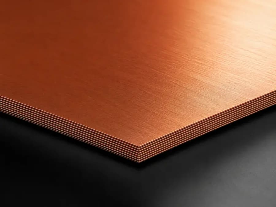
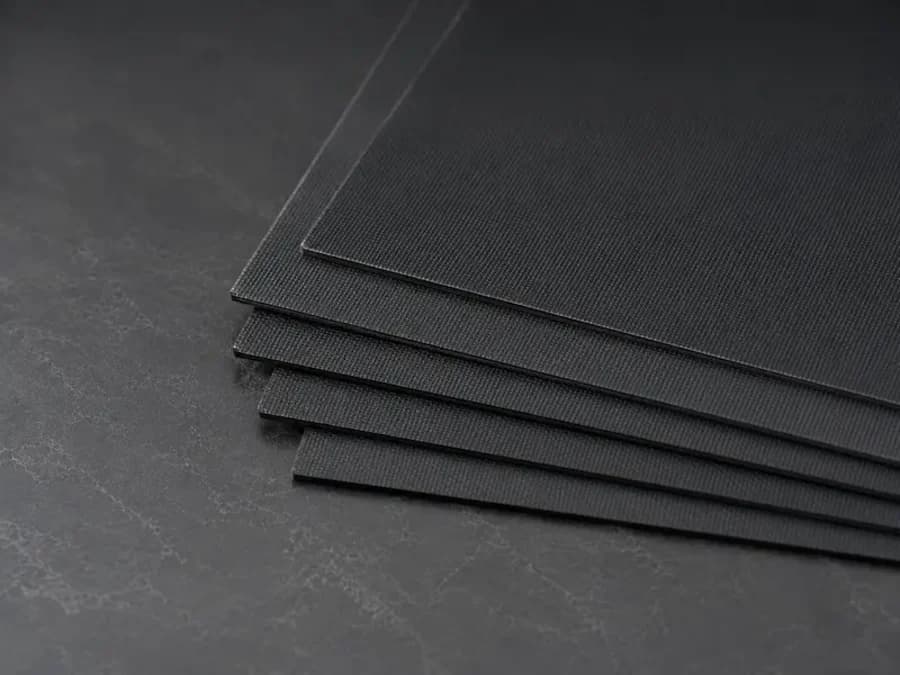
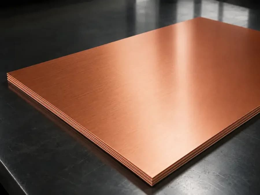
PTFE, hydrocarbon-ceramic and composite material systems matched to your dielectric and thermal targets before a single panel is cut.
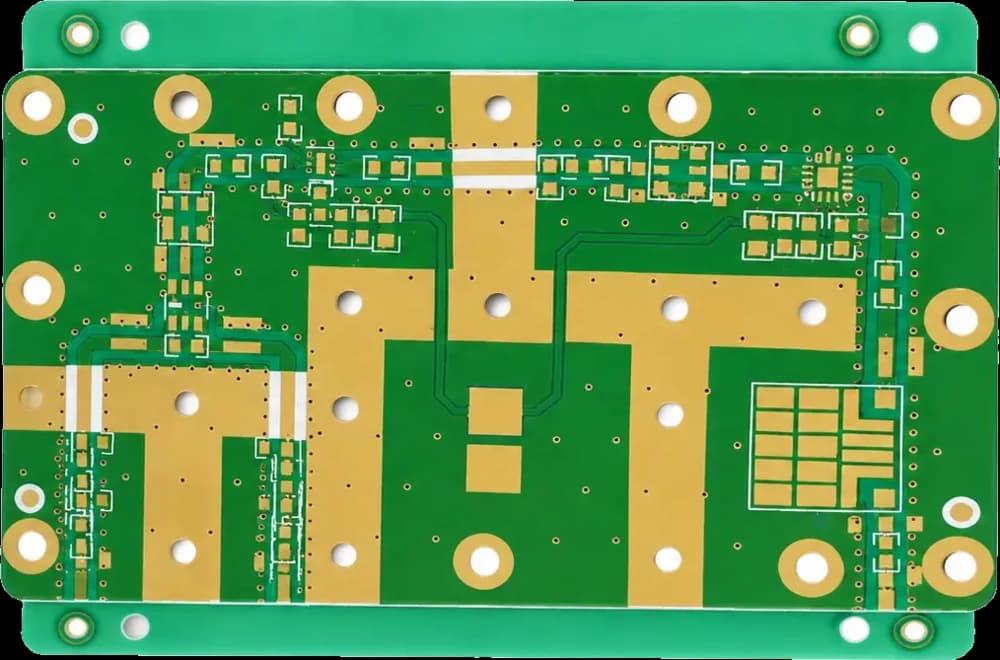
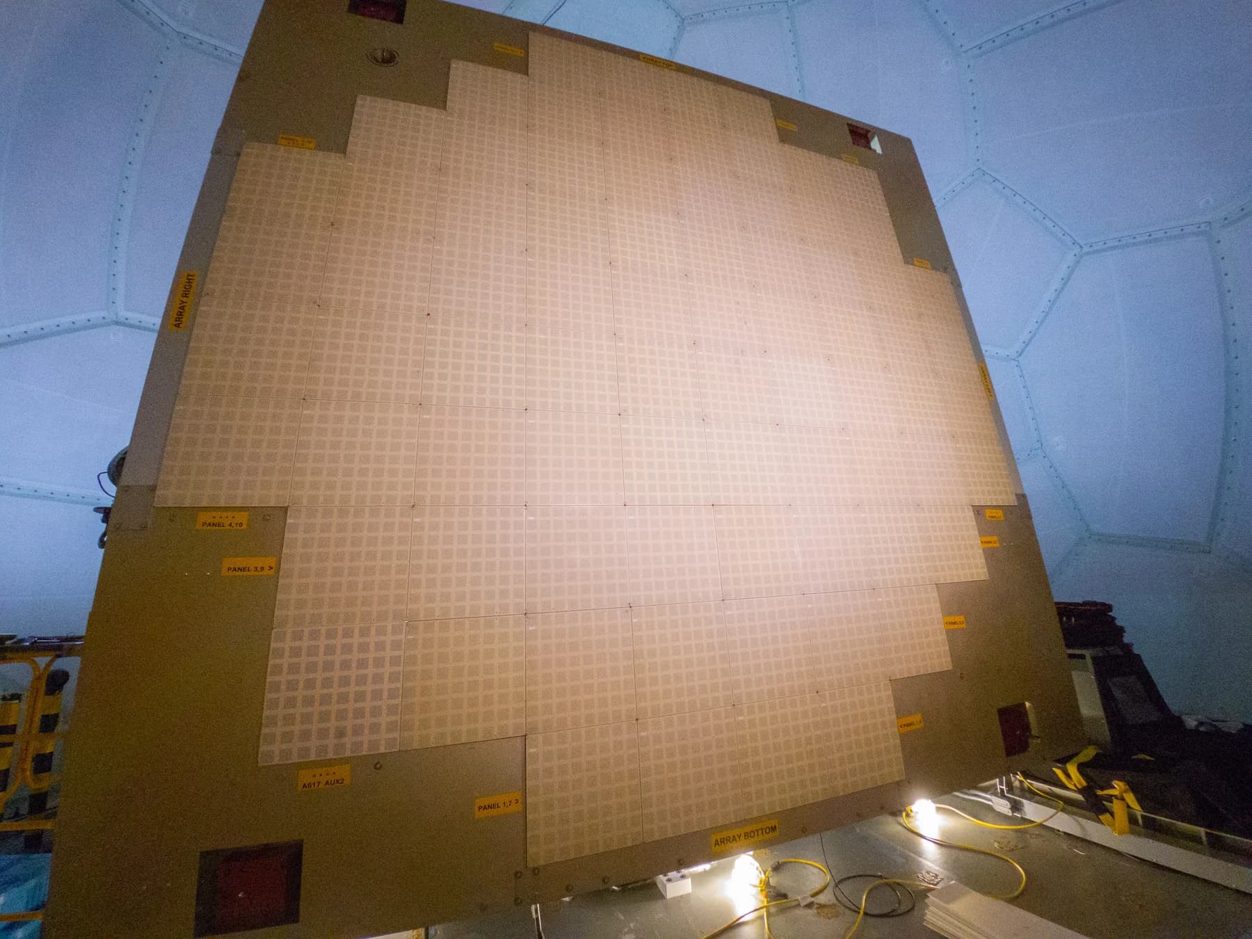
High-frequency laminates and finished PCBs manufactured in-house — one vertically integrated path from raw substrate to tested board, verified to 40 GHz.
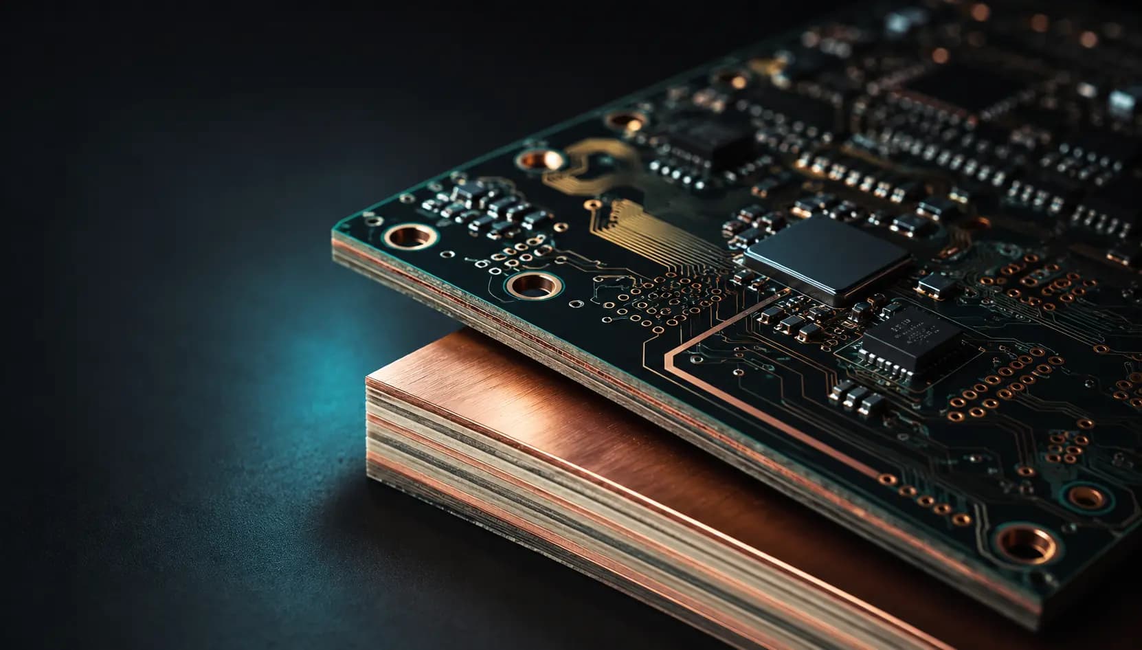
Material behaviour defines RF performance. Engineering the laminate and fabricating the board inside the same system removes substitution risk, handoffs and delay.
PTFE, hydrocarbon-ceramic and composite material systems matched to your dielectric and thermal targets before a single panel is cut.
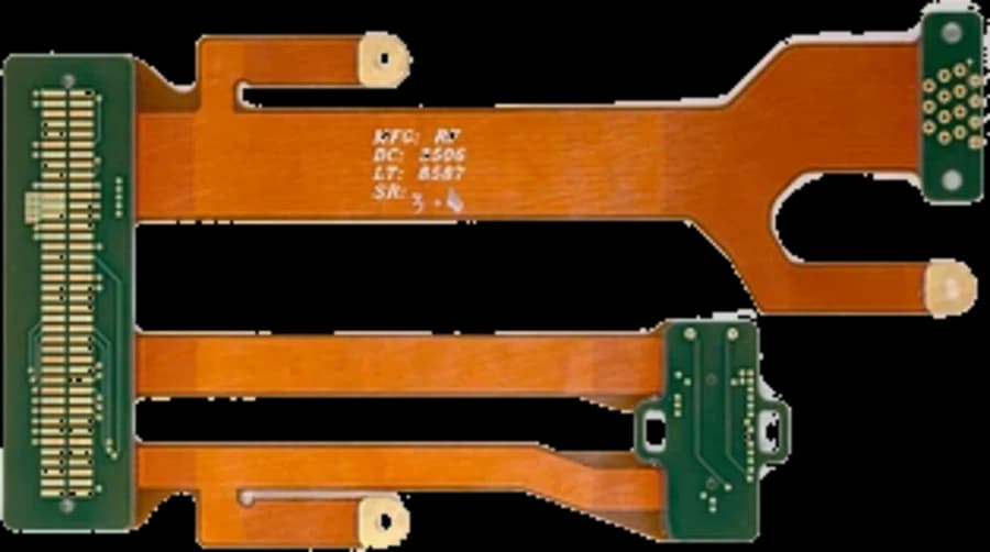
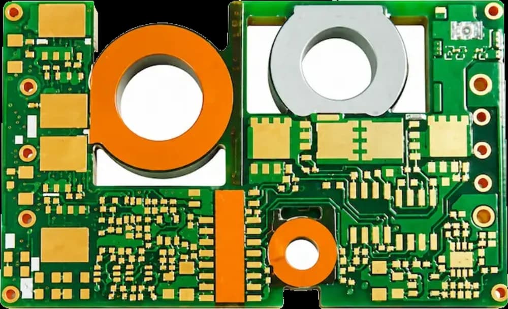
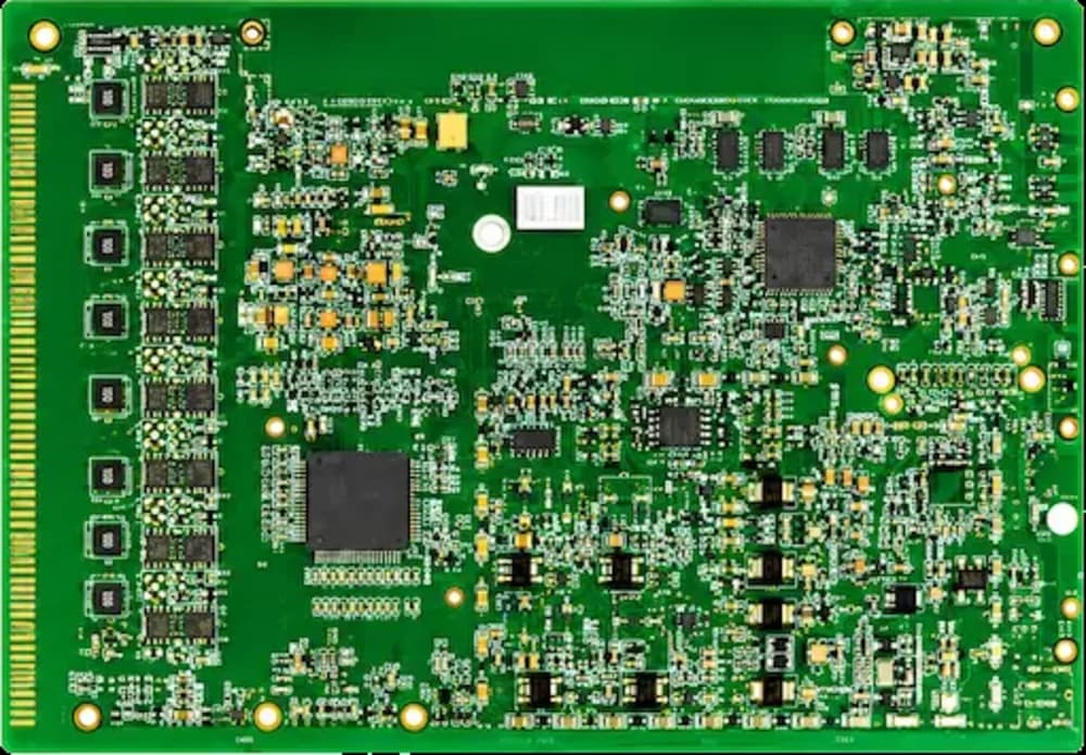
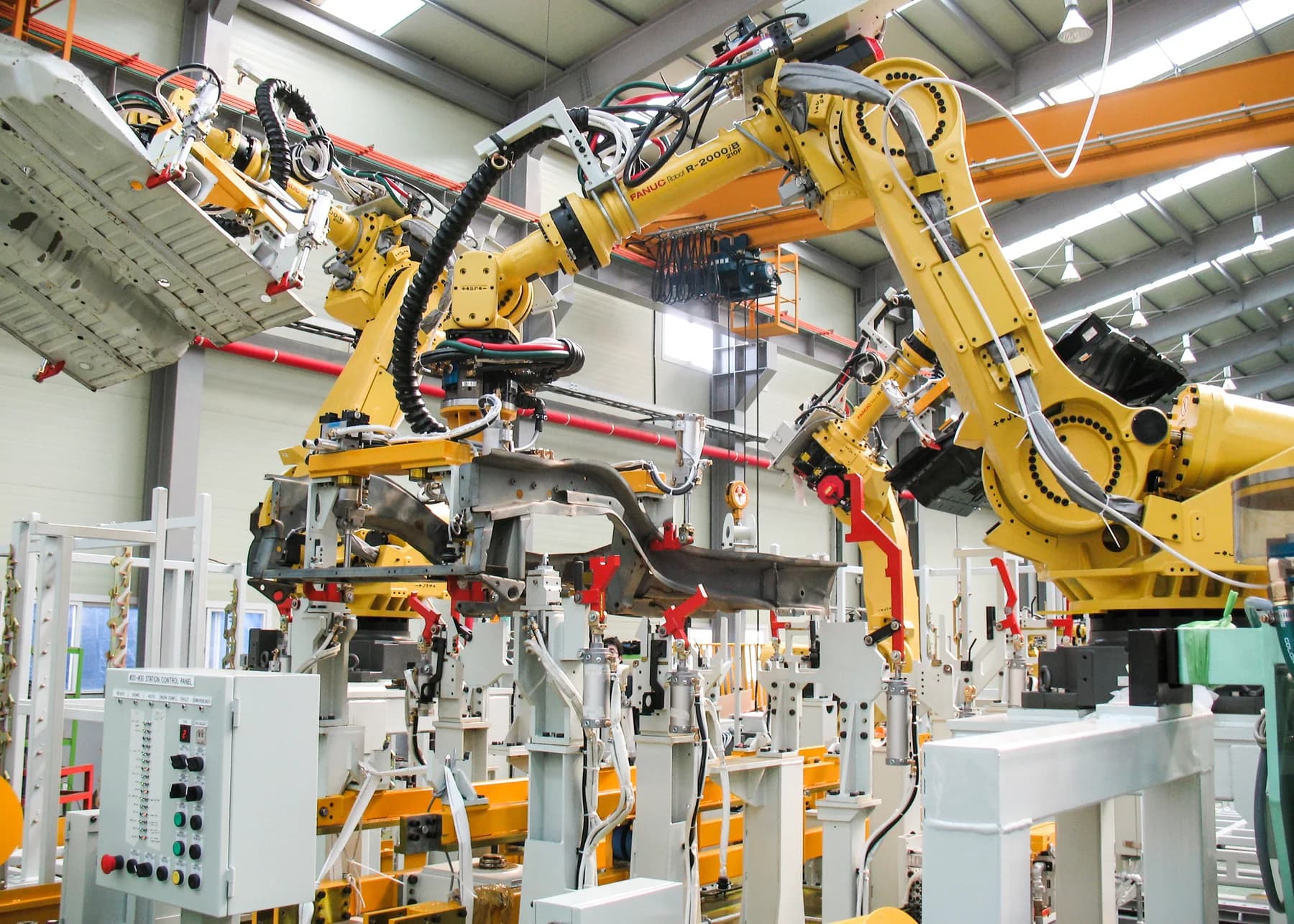
Laser direct imaging, laser microvias, vacuum lamination and controlled copper plating across RF, HDI and complex multilayer builds.
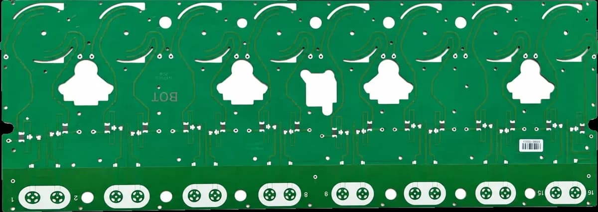
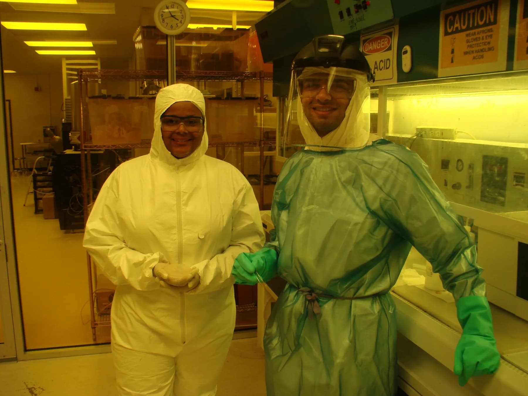
AOI, 3D X-ray, electrical and TDR verification, with revision control and material traceability from prototype through production.
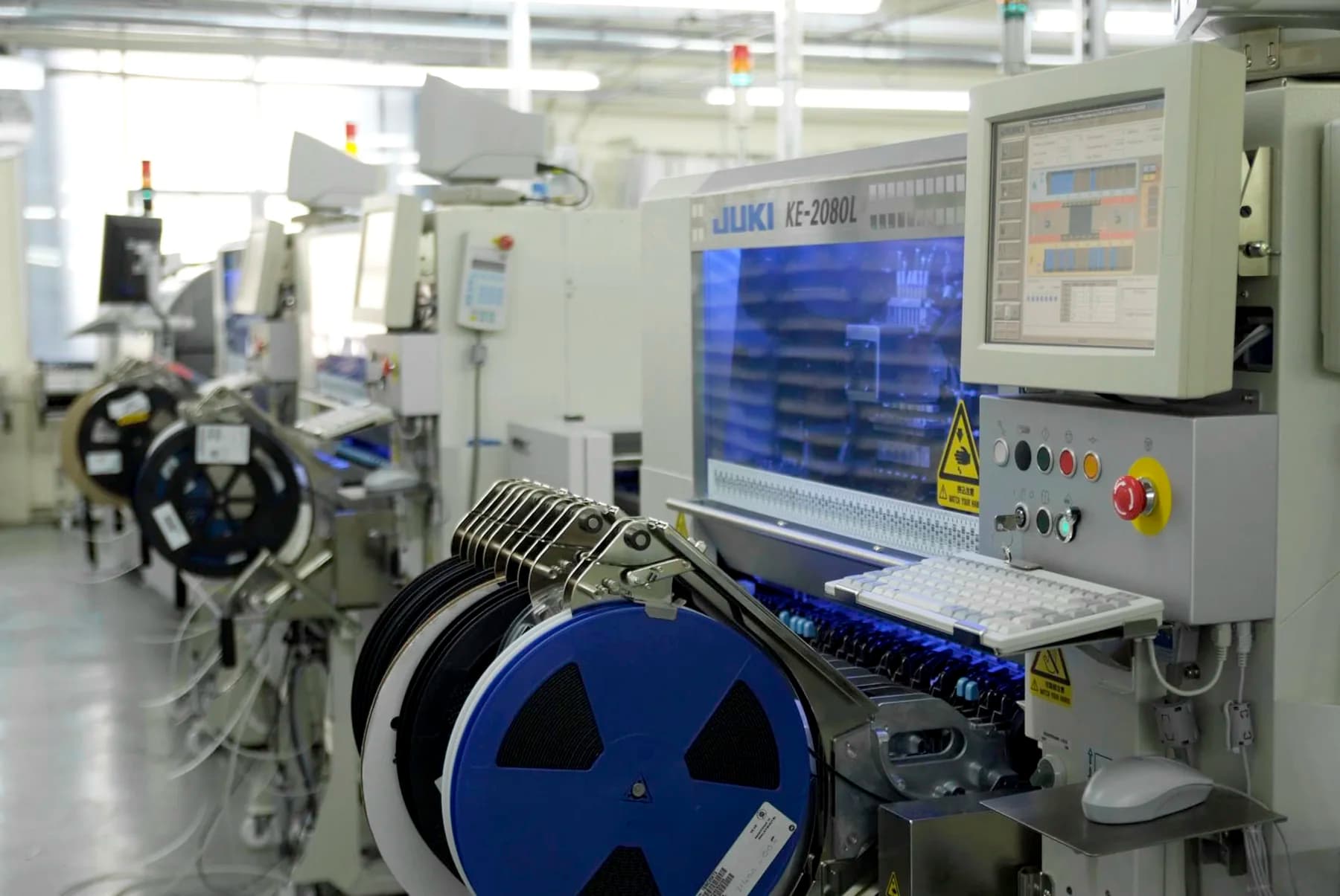
Dielectric coverage from Dk 2.17 to 10.2, fabricated in-house — factory-direct datasheets, and usually better pricing than premium import grades.
Fig. 01Four-layer stack-up on a PTFE core: laser microvia from L1 to L2, plated through hole across the full board, prepreg bonding either side.
Dk/Df tables and Tg values come straight from the plant that presses the panel — ask and we send the datasheet.
| Family | Key property | Substrates | Typical use |
|---|---|---|---|
| Bonding Sheets & Composite Substrates | Prepreg 0.05 – 0.3 mm | Prepreg, Composite | Microwave circuits needing practical electrical and process behaviour |
| High-Frequency & RF Laminates | Dk 2.17 – 10.2 | PTFE, Hydrocarbon-Ceramic, Composite | Low-loss antenna boards and RF feeder structures |
| Hydrocarbon Ceramic RF Laminates | Dk 3 – 10.2 | Hydrocarbon-Ceramic | RF front-end boards where cost and performance must balance |
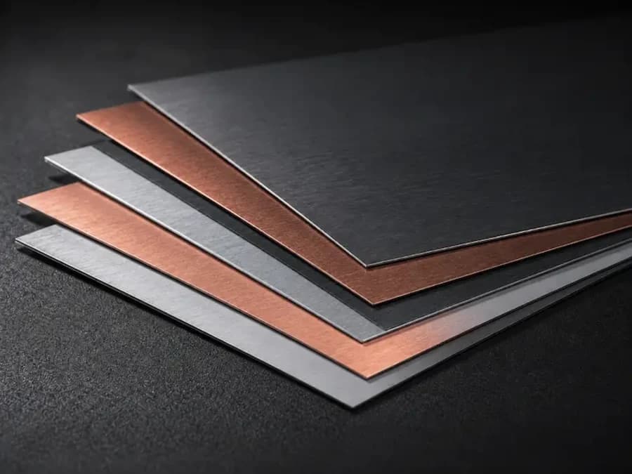
| Metal Core & Thermal Management Laminates | 1 – 6 W/mK | Aluminum Core, Copper Core | LED lighting and high-power LED modules |
Defense-grade production discipline is applied to commercial and mission-critical orders alike — measurable controls, verified records and direct engineer-to-engineer communication. Signal integrity is verified to 40 GHz.
Inner & outer layer AOI
Active3D X-ray via verification
ActiveTDR impedance testing
ActiveElectrical test & records
ActiveCertified to
10 standards · audited annually
 IATF 16949:2016Automotive quality management system for series and service part production.
 IECQ QC 080000Hazardous substance process management for RoHS and REACH compliant manufacturing.
 IPC Class 2/3Workmanship acceptance to IPC-A-600 and IPC-6012 Class 2 and Class 3, specified per order.
 ISO 13485:2016Quality management system for the design and manufacture of boards used in medical devices.ISO 14001:2015Environmental management system for manufacturing operations, chemical handling and waste treatment.ISO 45001:2018Occupational health and safety management system across production and chemical process areas.ISO 9001:2015Quality management system covering PCB fabrication, laminate manufacturing and assembly.
 REACHRegistration, evaluation and authorisation of chemical substances used in production.
 RoHSRestriction of hazardous substances in finished boards, finishes and assembly materials.
 UL VerifiedFlammability and material verification for laminates and finished boards.
One engineering path carries stack-up decisions, material records and inspection requirements from R&D validation into production.
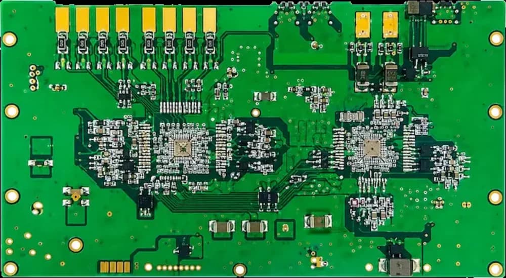
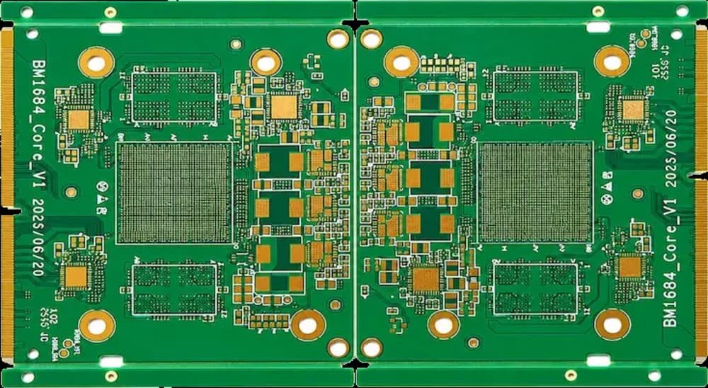
Aerospace, defense, medical and automotive programmes — the documentation package is as production-ready as the boards.
Upload your Gerber files for a secure review. An engineer returns a DFM assessment and a precise quote within 24 hours.
HyperPCB AI
Engineering assistant
Online · pre-sales
Ask about materials, stack-ups and tolerances — or what to send so a quote comes back in 24 hours.
AI pre-sales · an engineer confirms every quote