— CAPABILITIES
PCB Reverse Engineering Capability
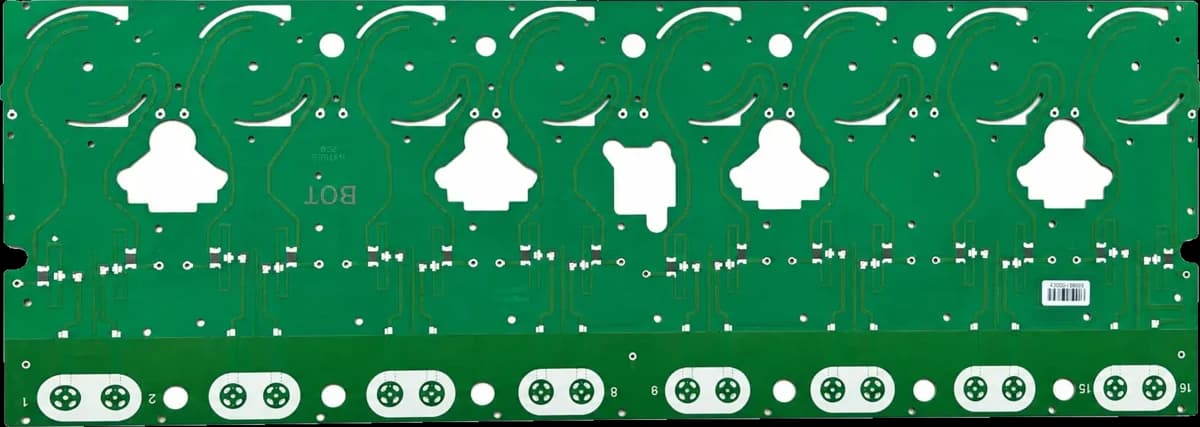
HyperPCB reconstructs manufacturing data for legacy or undocumented boards — layer extraction, netlist recovery, stack-up and material identification — and returns a buildable Gerber and drill package with a first article for comparison.
— SPECIFICATIONS
Capability & tolerance chart
| Parameter | Standard |
|---|---|
| Input Accepted | Bare board or populated assembly, partial documentation, film or paper artwork |
| Layer Extraction | Up to 48 layers |
| Output Package | Gerber RS-274X or ODB++, drill files, stack-up, netlist |
| Material Identification | Dielectric thickness, Dk estimate, copper weight |
| Netlist Verification | Electrical test against the recovered netlist |
| First Article | Built and compared to the original sample |
Recovering data, not guessing at it
Layers are imaged and cross-sectioned to measure dielectric thickness and copper weight, the netlist is extracted and verified electrically against the original board, and impedance-critical nets are modelled from the measured stack-up. The deliverable is a manufacturing package another fabricator could read, not a set of images.
What you should tell us first
Whether the board must be electrically identical or only mechanically compatible, whether components can be desoldered, how many samples you can release, and whether the design must move to RoHS-compliant materials. Each answer changes the scope.
Ownership and confidentiality
We ask you to confirm you hold the rights to the board being reconstructed, and the work runs under a mutual NDA on isolated servers with no third-party access.
— FAQ
Frequently asked questions
— RELATED
Related capabilities
Ready to build?
Upload your Gerber files for a free DFM review and a quote within 24 hours. Mutual NDA available.