— SOLUTIONS
High-Frequency PCB Solutions
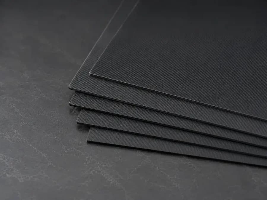
HyperPCB supplies high-frequency PCB solutions across Dk 2.17 to 10.2 with in-house PTFE and hydrocarbon-ceramic laminates, hybrid stack-ups and ±7% impedance control for communications, instrumentation and sensing products.
— SPECIFICATIONS
Capability & tolerance chart
| Parameter | Standard | Advanced |
|---|---|---|
| Dielectric Range | Dk 2.17 – 10.2 | — |
| Loss Performance | Low-Df PTFE and hydrocarbon-ceramic systems | — |
| Impedance Tolerance | ±10% | ±7% |
| Construction | RF-only, hybrid RF/FR-4, HDI on RF material | — |
| Verification | TDR impedance testing with report | — |
Pick the dielectric from the requirement, not the catalogue
High Dk shrinks a resonator; low Df protects a link budget; a stable thermal coefficient keeps a filter in band across temperature. These pull in different directions, so we start from the parameter that must not move and work back to a material we can fabricate consistently.
Supply continuity
Material substitution mid-programme is one of the most expensive events in RF production. Fabricating the laminate ourselves removes the third-party allocation risk and keeps the qualification you paid for valid.
— FAQ
Frequently asked questions
— RELATED
Related solutions

Ready to build?
Upload your Gerber files for a free DFM review and a quote within 24 hours. Mutual NDA available.