— SOLUTIONS
Multilayer PCB Solutions
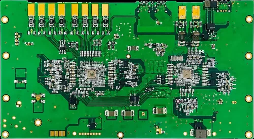
HyperPCB supplies multilayer PCB solutions from 4 to 48 layers with stack-up engineering, ±7% controlled impedance, 20:1 aspect ratio through holes and 100% AOI on every layer — from first article to repeatable production.
— SPECIFICATIONS
Capability & tolerance chart
| Parameter | Standard | Advanced |
|---|---|---|
| Component Density | Low to moderate on 2-layer boards | High to very high on multilayer |
| Signal Speed | Below 100 MHz on simple builds | 100 MHz to 10+ GHz on controlled multilayer |
| EMI Control | Minimal shielding on simple builds | Dedicated reference planes and built-in shielding |
| Routing | Simple routing | Complex routing across many layers |
| Cost Behaviour | Lower unit cost | Higher unit cost, lower cost per function |
| Layer Count | 4 – 48 layers | — |
| Impedance Tolerance | ±10% | ±7% by stack-up review |
Stack-up engineering included
Send a layer count and an impedance target and you get a proposed stack-up with the dielectric thicknesses, copper weights and modelled trace widths spelled out. It is easier to argue about a model than to debug a finished board.
From first article to volume
Prototypes run on the production process, then the stack-up, material lots and inspection requirements are frozen under revision control so the tenth build matches the first.
— FAQ
Frequently asked questions
— RELATED
Related solutions

Ready to build?
Upload your Gerber files for a free DFM review and a quote within 24 hours. Mutual NDA available.