— SOLUTIONS
RF & Microwave PCB Solutions
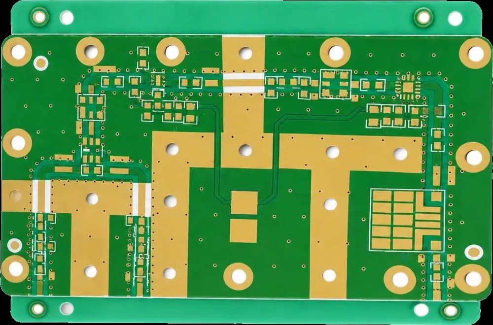
HyperPCB builds RF and microwave PCBs for antennas, radar, satellite links and RF front-ends on laminates it fabricates itself — Dk 2.17 to 10.2, impedance held to ±7%, signal integrity verified to 40 GHz.
— SPECIFICATIONS
Capability & tolerance chart
| Parameter | Standard | Advanced |
|---|---|---|
| Frequency Range | Verified to 40 GHz | — |
| Dielectric Constant | Dk 2.17 – 10.2 | — |
| MaterialsAll fabricated in-house | PTFE, hydrocarbon-ceramic, composite | — |
| Impedance Tolerance | ±10% | ±7% |
| Typical Builds | 2 – 20 layers, RF-only and hybrid RF/FR-4 | — |
| Surface Finish | ENIG, ENEPIG, immersion silver | — |
Antenna and radar front-ends
Patch arrays, feed networks and radar front-ends live or die on dielectric consistency across the panel. Because the laminate is ours, batch-to-batch Dk variation is a number we measure rather than a specification we inherit, which is what keeps beam patterns repeatable between production lots.
Where hybrid construction wins
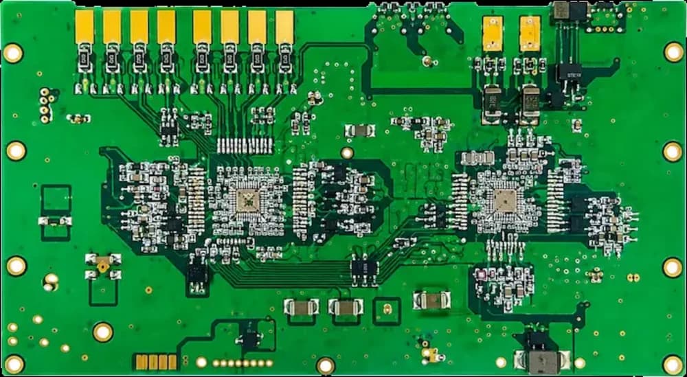
A transceiver board rarely needs low-loss material on every layer. Bonding two or three RF layers to FR-4 cores holds the RF budget while the digital section stays conventional and affordable. We model the hybrid stack-up and state the bond system before quoting.
What to send
Operating band, target impedance and tolerance, the loss budget if you have one, and which layers carry controlled lines. We return a stack-up with modelled trace widths and the measured Dk of the material we will build on.
— FAQ
Frequently asked questions
— RELATED
Related solutions

Ready to build?
Upload your Gerber files for a free DFM review and a quote within 24 hours. Mutual NDA available.